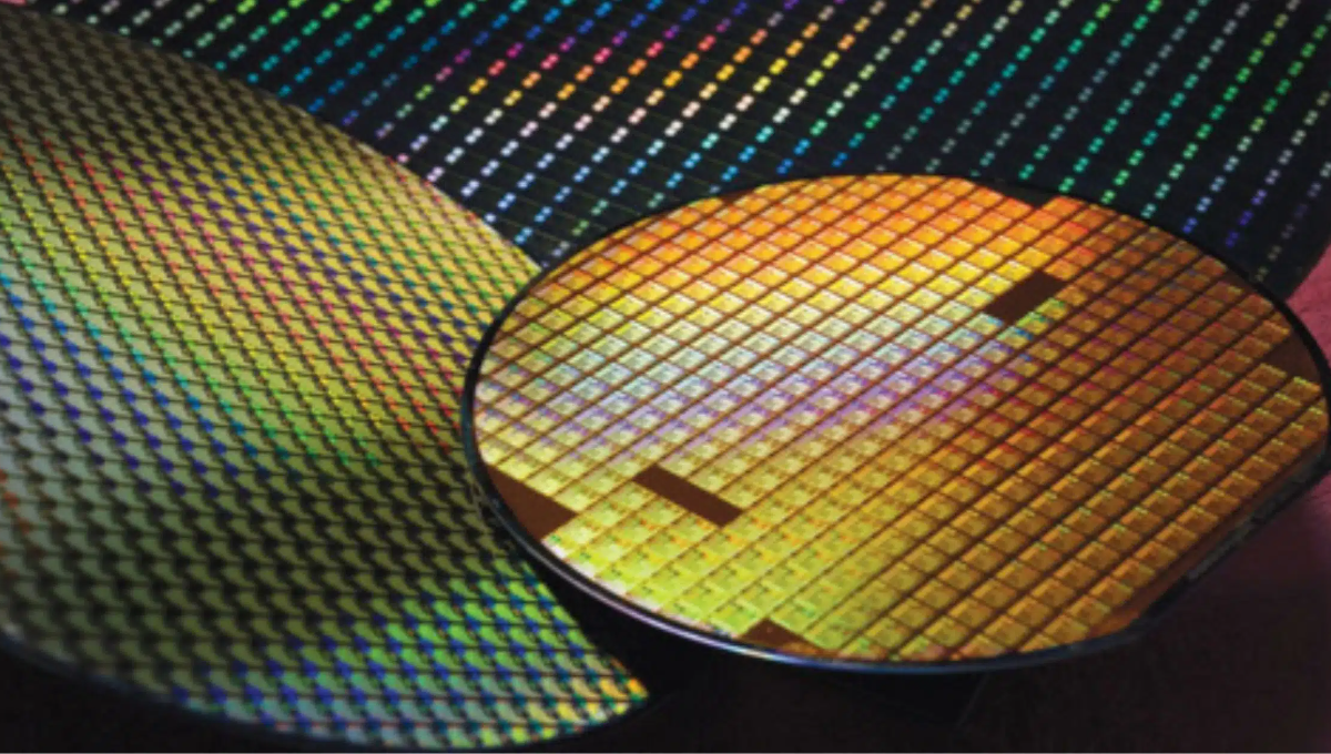
Cadence Design Systems has entered a collaboration with TSMC to create advanced design solutions and semiconductor IP aimed at accelerating the development of next-generation chips for high-performance computing. The partnership focuses on cutting-edge process nodes and 3D-IC packaging technologies to streamline the chip development cycle.
The companies announced that Cadence’s design automation workflows are now compatible with TSMC’s N2 and A16 technologies. Additionally, new silicon-verified IP has been developed for the N3P node. Both firms are also co-developing design flows for TSMC’s upcoming A14 process, with its initial Process Design Kit (PDK) expected later this year.

Cadence has expanded its suite of automation tools to cover TSMC’s latest fabrication technologies, including N3, N2, and A16. These enhancements ensure that engineers working on cutting-edge chips have access to optimized tools tailored to the demands of modern semiconductor manufacturing.
Solutions such as the Innovus Implementation System, Tempus Timing Solution, and Voltus IC Power Integrity Solution are now integrated with TSMC’s workflows. These tools will allow developers to fine-tune designs for better power efficiency, performance, and chip density — key metrics for computing-intensive applications.
Chin-Chi Teng, senior vice president and general manager at Cadence, emphasized the shared commitment between the two companies to improve and accelerate the design cycle for complex silicon. By working together, the companies aim to reduce the time and cost it takes to bring high-performance chips to market.

TSMC’s Aveek Sarkar, who leads ecosystem and alliance management, noted that the collaboration is focused on overcoming the increasing complexity of semiconductor design while improving energy efficiency and computing performance. TSMC has successfully verified Cadence’s JedAI and Cerebrus tools, which help automate tasks like design rule correction to speed up chip completion.
Cadence’s 3D-IC solutions have also been updated to support TSMC’s 3DFabric packaging technologies. New features now include automation for bump connection management, physical integration of multiple chiplets, and smart marker insertion to assist with precise alignment — all crucial for advanced multi-die systems.
On the intellectual property front, Cadence introduced new memory and connectivity solutions developed on TSMC’s N3P process. These include support for next-generation standards such as HBM4, LPDDR6/5X, DDR5 MRDIMM Gen2, PCIe 7.0, and UCIe 32G. These innovations aim to address growing data bandwidth demands and help developers build scalable compute infrastructures.
Also Read:
OpenAI ramps up developer push with more powerful models in its API